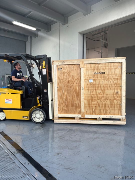
In late June, a truck pulled up to NeoCity and unloaded a heavy box — over 900 pounds. The impressively sized delivery was met with excitement by businesses at NeoCity.
Bridg Vice President of Marketing and Communications Gloria LeQuang said the contents of that box point to a future where NeoCity attracts more semiconductor manufacturing and advanced packaging to the region. Bridg is an economic growth nonprofit that communicates on behalf of all NeoCity businesses.
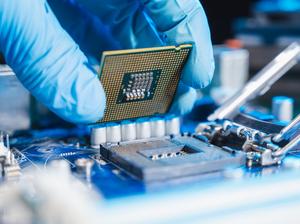
The delivery was a D9650 C-SAM, an acoustic microscope that inspects bonded wafers — thin slices of semiconductor — for defects. The tool and its accessories cost $264,496 and came from Nordson Test & Inspection Americas, according to a Bridg representative. The C-SAM's acoustic microscope allows manufacturers to more efficiently and effectively check the products it makes for defects, which ultimately saves money, said Bridg President James Vandevere.
The C-SAM is one purchase made possible by a grant from the U.S. Economic Development Administration. According to LeQuang, the equipment will be maintained by SkyWater Florida once it is installed, and NeoCity programs requiring tool capabilities will have access to it under SkyWater supervision. SkyWater is a semiconductor manufacturer based in Bloomington, Minnesota, and the company has a footprint at NeoCity under the name SkyWater Florida.
Why this matters: To attract more semiconductor manufacturing business to NeoCity, more leading-edge tools — like the C-SAM — are needed. NeoCity leaders plan to use grant money to buy tools that make NeoCity a competitive location for semiconductor business, in which access to expensive, sophisticated tools is essential.
In September 2022, a coalition that includes Osceola County, Orlando Economic Partnership, the University of Central Florida, Bridg, the Florida High Tech Corridor, SkyWater Technology (Nasdaq: SKYT) and the Osceola Chamber was awarded $50.8 million through the U.S. Economic Development Administration’s Build Back Better Regional Challenge. Buying the C-SAM is one of many commitments made by the coalition in its application for the award.
So, what is a wafer?
Many people may be hard-pressed to define a wafer, but it is a key element for those who love smartphones and video games. A wafer is the silicone foundation for integrated circuits of miniaturized transistors and other electronic components. An integrated circuit bonded to layers of wafers is a microchip, according to the website of ASML, a company that makes tools for the semiconductor industry.
Microchips make computers, smartphones, appliances, gaming hardware and some medical equipment function in the ways people have grown to expect, and that’s just scratching the surface. The more people look to objects to be smart, the more they rely on microchips.
For the user experience to be flawless, bonded wafers with all the tiny electronics inside need to be flawless. That means no air pockets, for example. Checking to make sure the bonded wafers are flawless can be a tedious task.
Vandevere shared this analogy: “I thought about it while I was making pancakes on Sunday. So you take a pancake and put butter on it. Then you take another pancake and put it on top of the butter that's on top of the other pancake and press it down so the butter spreads evenly. But then you're like, wait a second, how do I know I put enough butter on there? And the only way to know is to take them apart.”
Today, it’s a common best practice to employ sophisticated wafer inspection tools like the D9650 C-SAM, said Vandevere. The old way, which involved slicing bonded wafer stacks at the bond line and opening them up to look for flaws led to breakage. It was cumbersome and inefficient.
Semiconductor technology is becoming ever more complicated, according to the Institute of Electrical & Electronics Engineers. The membership organization’s website notes that artificial intelligence, the Internet of Things, and growing semiconductor technologies have sparked a new wave of innovation in the semiconductor industry.
The more complicated the digital elements of a project, the more challenging it is to ensure quality, so a sophisticated tool that can detect gaps in the bond that holds wafers together is important to production at NeoCity.
Sign up here for The Beat, Orlando Inno’s free newsletter. And be sure to follow us on LinkedIn, Facebook and Twitter.